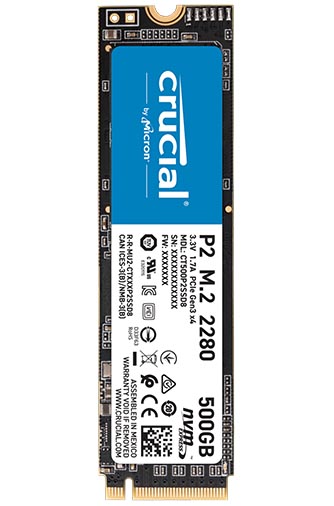
Crucial P2
SSD Specification and Info
Crucial P2 is an Entry-Level NVMe SSD produced and sold by Crucial. The device comes with x4 PCIe 3.0/NVMe interface and M.2 form factor - a good fit for both desktop and laptop computers. This SSD has a maximum sequential read-write speed of up to 2400/1900 MB per second, making it ideal for gaming and workstation PCs.
Due to its lack of DRAM memory, Crucial P2 has slight disadvantages over SSDs with DRAM memory. This SSD is using a TLC NAND flash memory with 96 cell layers.
NAND type
Crucial P2 is using a TLC (3 bits per cell) NAND manufacurted by Micron with 96 cell layers on top of each other.
The TLC is the most common type of SSD NAND flash memory found on the market at the moment. It is faster, less durable, but still cheaper than the other, more expensive variants - SLC and MLC.
The main advantage of this type of NAND chips is the fact that the cost per gigabyte is much lower, allowing high capacity SSDs at affordable price.
The Controller
Crucial P2 is using Phison E13T SSD controller to connect the NAND memory to the x4 PCIe 3.0/NVMe interface. The controller has Single-core, 4-ch, 8-CE/ch configuration.
Typically, SSD controllers are microprocessors. In this case we have Single-core, 4-ch, 8-CE/ch processor responsible for controlling the SSD in such way, so that the data coming from the interface can be stored on to the NAND flash memory.
Some SSDs have simpler controllers with fewer communication channels and less cores.
Among other things, the controller also manages the SLC caching, optimizing the DRAM cache, encryption, LDPC, garbage collection, wear-leveling as well as TRIM
DRAM Cache
Crucial P2 has no separate DRAM chip to store the SD mapping tables to speeds up the data access.
As soon as the OS requests some data from the SSD, the SSD needs to know exactly where it is on the drive. Because garbage collection moves the data constantly, the controller relies on the mapping tables to locate it.
These tables are stored in DRAM cache, where they are accessed much more quickly than in NAND flash.
Therefore, SSDs with DRAM-less architecture have more random write and read operations. This makes the device perform worse and last shorter if they are not HMB enabled.
HMB Support
Crucial P2 has a DRAM-less architecuter and it is using a host memory buffer (HMB) to store the mapping tables.
The HBM is used to reduce the cost of production of NVMe SSDs with DRAM Cache, SSDs with this type of controllers can leverages the host system's DRAM instead of an onboard DRAM chip to host the FTL mapping table used by flash storage.