For years, the formula for running large language models locally has been simple: get as much VRAM as you can afford. This usually meant building complex, power-hungry desktop rigs with multiple GPUs or hunting for deals on used server hardware. But a new class of hardware, powered by Apple Silicon and AMD’s “Strix Halo” APUs, is challenging that assumption. These compact, power-efficient chips can handle surprisingly large models, and the secret isn’t just raw compute power. It’s all about memory.
These systems use a fundamentally different approach to memory architecture that delivers massive bandwidth and capacity in a small package, making them uniquely suited for the demands of LLM inference.
Unified Memory and the Wide Bus
The core technology enabling this leap is a Unified Memory Architecture, or UMA. In a traditional PC, the CPU has its system RAM, and a discrete GPU has its own dedicated, high-speed VRAM. For an LLM, the model’s weights must live in one of these pools, usually the VRAM. If a model is too big, you need more VRAM, which gets expensive fast.
Apple’s M-series chips and AMD’s Strix Halo throw this design out. They put the CPU, GPU, and Neural Engine on a single piece of silicon, a System-on-a-Chip (SoC), and give them all access to one shared pool of high-speed memory. This eliminates the need to copy data between CPU and GPU memory, but more importantly, it allows for a memory interface that is physically impossible in a standard desktop.
Because the memory chips are soldered extremely close to the SoC, the electrical pathways are incredibly short. This signal integrity allows engineers to design memory buses that are two to four times wider than a typical desktop’s. While a standard dual-channel DDR5 desktop PC has a 128-bit memory bus, these SoCs boast buses that are 256-bit, 384-bit, or even wider. For LLM inference, which is often bound by how fast you can feed model weights to the compute cores, this wider bus is the key to performance.
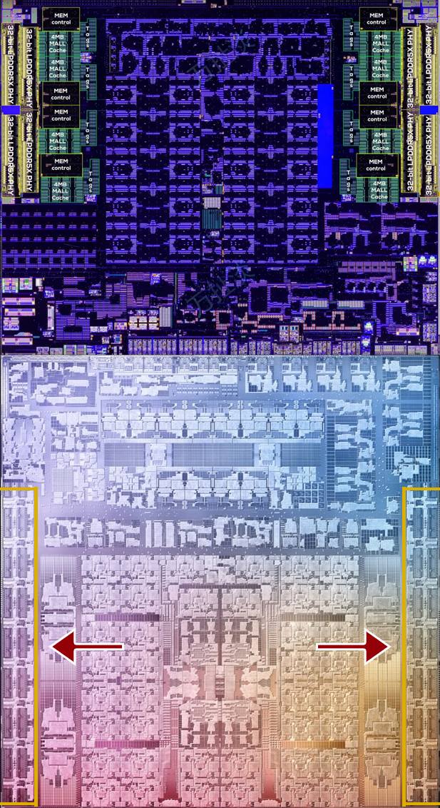
Die comparison between Apple’s M4 Max and AMD’s Strix Halo: the M4 Max (bottom) features a massive 512-bit LPDDR5X memory bus (32 x 16-bit controllers), delivering up to 546 GB/s of bandwidth, while Strix Halo (top) uses a 256-bit interface (8 x 32-bit PHYs) with LPDDR5X, balancing efficiency and bandwidth for its integrated GPU and NPU.
While both chips use LPDDR5X memory, their connection topologies differ significantly. Apple’s M4 Max integrates a 512-bit memory interface composed of 32 × 16-bit controllers, all running at 8,533 MT/s. Because LPDDR memory transfers two bytes per pin per cycle, total theoretical bandwidth is calculated as:
(8,533 × 10⁶ × 512 ÷ 8) = ≈546 GB/s.In contrast, AMD’s Strix Halo employs a 256-bit LPDDR5X interface, implemented as 8 × 32-bit PHYs distributed around the SoC. At 8,000 MT/s, this yields a peak bandwidth of about:
(8,000 × 10⁶ × 256 ÷ 8) = ≈256 GB/s.This physical difference is clearly visible in the die layout: the M4 Max’s on-package memory connections enable shorter traces and higher signaling integrity, while Strix Halo’s off-package LPDDR configuration trades a narrower bus for more flexible manufacturing and cost efficiency.
How They Achieve Massive Bandwidth
This impressive bandwidth is not magic; it is a direct result of the physical design. Instead of using socketed, user-replaceable DIMM modules, these systems use Low Power Double Data Rate (LPDDR) memory chips soldered directly to the hardware.
LPDDR memory is designed for mobile applications, prioritizing efficiency and speed over short distances. This allows for a more compact design and lower power consumption compared to its desktop DDR counterpart.
| Feature | Standard PC (Dual-Channel DDR5) | SoC (LPDDR5X) |
| Physical Form | Socketed, user-replaceable DIMMs | Soldered chips on package or board |
| Total Bus Width | 128-bit (2 x 64-bit channels) | 256-bit to 512-bit |
| Typical Bandwidth | ~96 GB/s (DDR5-6000) | 256 GB/s to 800+ GB/s |
| Primary Goal | Flexibility and user choice | Maximum performance and efficiency |
AMD’s Strix Halo achieves its 256-bit bus by placing eight 32-bit LPDDR5X memory chips on the motherboard, surrounding the main SoC. Apple takes this a step further, placing its memory chips on the same physical package as the SoC itself, a design called Memory-on-Package (MoP). This makes the connection distance even shorter, enabling the truly massive bus widths seen on the M-series Max and Ultra chips.
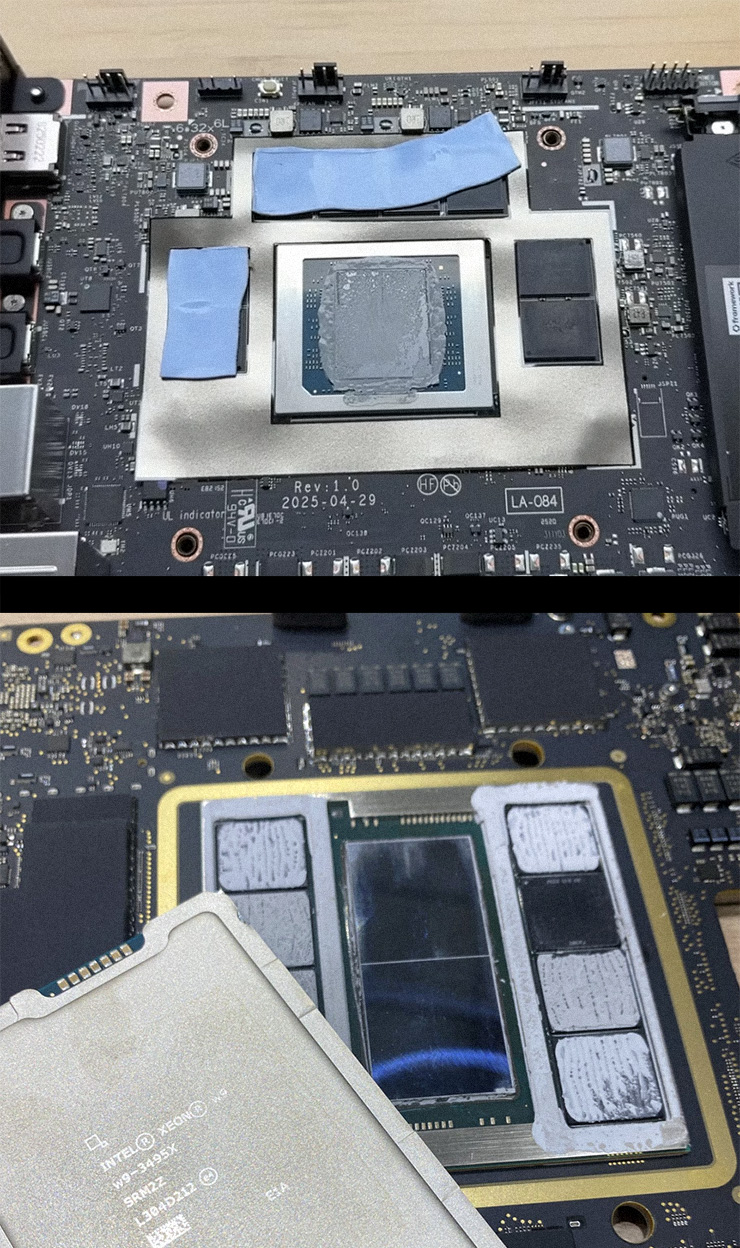
Top: AMD Strix Halo on a laptop mainboard with eight external LPDDR5X memory packages surrounding the SoC. Bottom: Apple M2 Ultra featuring on-package LPDDR5X memory chips tightly integrated beside the die, highlighting the 256-bit vs. 512-bit bus architecture difference.
Apple Silicon vs. AMD Strix Halo
Both Apple and AMD leverage this wide-bus UMA design, but their product lines offer different trade-offs in performance and price. Strix Halo aims to bring this architecture to the broader Windows laptop market, while Apple has been refining it for years across its product stack. The Pro, Max, and Ultra variants of Apple’s chips use progressively wider memory buses to feed their larger GPUs, offering incredible performance but at a significant price premium.
Here is a look at the memory specifications for these high-performance SoCs.
| Chip Family / Model | Memory Type | Bus Width | Peak Bandwidth | Max Memory |
| AMD Ryzen AI 9 HX 370 (Strix Halo) | LPDDR5X-8000 | 256-bit | ~256 GB/s | 128 GB |
| Apple M1 Max / Ultra | LPDDR5-6400 | 512-bit / 1024-bit | ~409 GB/s / ~819 GB/s | 64 GB / 128 GB |
| Apple M2 Max / Ultra | LPDDR5-6400 | 512-bit / 1024-bit | ~409 GB/s / ~819 GB/s | 96 GB / 192 GB |
| Apple M3 Max / Ultra | LPDDR5-6400 | 512-bit / 1024-bit | ~409 GB/s / ~819 GB/s | 64 GB / 512 GB |
| Apple M4 Pro | LPDDR5X-8533 | 256-bit | ~273 GB/s | 24 GB – 64 GB |
| Apple M4 Max | LPDDR5X-8533 | 512-bit | ~546 GB/s | 36 GB – 128 GB |
Why This Matters for Local LLMs
This architecture directly addresses the two biggest pain points for local LLM users: memory capacity and memory bandwidth.
First, the capacity is enormous. A Strix Halo laptop can be configured with up to 128 GB of unified memory. For an LLM user, this is effectively 128 GB of VRAM. This allows you to run a 70-billion parameter model at a 4-bit quantization with plenty of room to spare, something that would otherwise require an expensive multi-GPU desktop setup or a high-end data center card.
Second, the bandwidth directly translates to faster token generation speed. Running a large model on a CPU with standard DDR5 memory results in slow inference because the ~96 GB/s bus becomes a bottleneck. With bandwidths from 256 GB/s to over 500 GB/s, these SoCs can feed their compute engines much faster, resulting in a more responsive and usable experience.
The Important Caveats
This architecture is not a silver bullet. While it excels at token generation (inference), which is bandwidth-bound, it is less impressive at initial prompt processing. That first ingest of a long context is a raw compute task, and a high-end discrete GPU like an RTX 4090 will still process it much faster. For users who prioritize inference speed and model size in a compact, efficient form factor, the trade-off is often well worth it.
The Future is Wider: Medusa Halo and LPDDR6
The trend of wider memory buses is set to continue. Future APUs, codenamed “Medusa Halo,” are rumored to adopt the LPDDR6 memory standard and expand the bus to 384-bits. LPDDR6 uses an unconventional 24-bit chip interface, meaning a 384-bit bus would require sixteen chips working in parallel.
Combined with the higher data rates of LPDDR6, this future 384-bit architecture could deliver between 514 GB/s and 691 GB/s of memory bandwidth. This level of performance rivals high-end discrete graphics cards, promising to make local inference of even larger and more capable models a reality in a standard laptop form factor. For the price-conscious hardware enthusiast, this new wave of SoCs represents a powerful and efficient alternative to the traditional VRAM chase.